Read Bitline Sensing and Fast Local Write-Back Techniques in Hierarchical Bitline Architecture for Ultralow-Voltage SRAMs
₹4,500.00
10000 in stock
SupportDescription
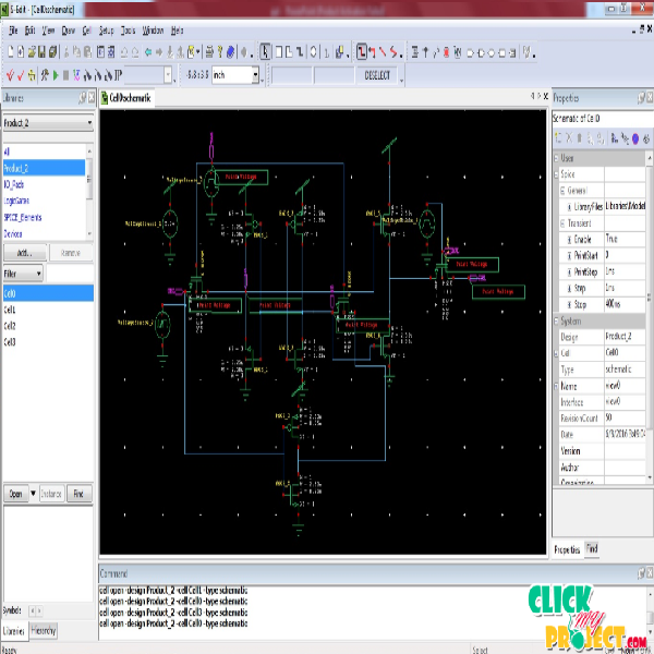
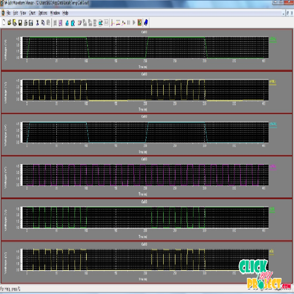
It is necessary to ensure any leakages which cause the read sensing failure and degraded cell stability due to the half-select write. For avoid this situation proposes an equalized bit line scheme to eliminate the leakage dependence on data pattern and thus improves RBL sensing. Also we propose a fast local write-back (WB) technique to implement a half-select-free write operation. With hierarchical bit line architecture, it facilitates a local read and a subsequent fast WB action to secure the original data without performance degradation. Here, we propose a design of low power SRAM architecture using CMOS technology. The proposed memory CMOS design is based on Swapped MOS technology. Our work, the proposed system is to design of 6T, 8T, 10T with sleep transistor based data storage architecture. Then to optimize the data storage devise and to reduce the power consumption. The portability in the electronic circuits are achieved by the use of battery. So we have make designs for low power consumption. As the technology in electronic circuits is improving, the complexity in the circuits also increases. The complexity in the circuits leads to the need of that type of circuits which are portable and fast circuits. The SRAM design is used to reduce the power consumption level, during the read and write operation. In this architecture, our work is to design a 8*8 bit 6T-sram memristor with sleep transistor architecture design. This design is to reduce the circuit complexity level and power consumption level. Existing system is to design a 7T-sram memristor CMOS design is to modify the storage process. This design is to implement the multi threshold CMOS function. This existing function is to optimize the read and writing process for memristor storage unit and to reduce the overall leakage power level. Our proposed work is to design the 9T based SRAM architecture with sleep transistor technique and we design the 8 * 8 SRAM cell design. This sleep transistor design is reduce leakage power when these operate in “stand-by mode” due to inefficient passing of the voltages (pass-transistors property). Our proposed work is to reduce the power and circuit complexity level. This work is to reduce the overall transistor count for memory cell storage operation.


